Introduction: Sure,
cooling is a good
thing, but how much
cooling do we really need to be in that "sweet spot" for amateur,
ground-based
astrophotography. There are two
aspects to this argument that I would like to present separately, one
involving the signal to noise ratio (SNR), and the other involving
dynamic
range. The discussion involving the SNR is very straightforward
but still interesting. The dynamic range argument introduces a
new metric that may take some getting used to. Both discussions
(SNR and dynamic range) are accompanied by interactive graphs and Excel
spreadsheets that allow you to explore these topics in greater detail.
I. How
does cooling
affect the Signal to Noise ratio?
It is well known that CCD
chips generate thermal electrons at a given
rate known as the dark current, which is related to chip
temperature. The higher the chip temperature, the higher the dark
current. The dark current, like sky flux or object flux, is a
source of noise that must be considered when calculating the signal to
noise ratio. Below I will modify the standard signal to noise equation
discussed earlier to account for the
contribution of dark noise. In the resultant interactive graphs
(requiring Quicktime 7 or later), you will see that the effect of the
dark noise contribution becomes minimal when the chip is cooled to the
range of -15 to -20 C, assuming that your conditions are typical of
most ground based, amateur imagers. If
you want to skip the math, just drop down to section B below
(Interactive Graphs), but you will be
missing a lot of fun <g>.
1.
The
signal
to noise ratio per pixel for a single sub is usually expressed as
follows
(ignoring
the contribution from dark noise):
SNR = (Obj)*tsub /
sqrt[(Sky+Obj)*tsub
+ R2]
where SNR
= signal to noise ratio per pixel; Obj = object flux in
electrons/minute/pixel; Sky =
sky flux in electrons/minute/pixel; tsub = subexposure time
in
minutes; R = read noise in e RMS.
2. For the
purpose of this discussion, we want to include
dark noise in the analysis, so let's represent the dark current as D,
in electrons/minute/pixel (for instance).
The equation simply becomes:
SNR = (Obj)*tsub /
sqrt[(Sky+Obj+D)*tsub
+ R2]
3.
The dark current (D) doubles with a constant delta increase in
temperature, which we will call the doubling temperature (Td).
For most CCD chips this is around a delta of 6 degrees
centigrade. So if the dark current is 30 electrons per minute at
0 degrees, it would double to 60 electrons per minute at 6
degrees, 120 electrons per minute at 12 degrees, etc. Conversely,
if the CCD temperature decreases by a delta of 6 degrees C, the dark
current D would be cut in half. This kind of relationship is
analogous to exponential growth of bacteria in an environment that has
unlimited space and nutrients, or from an oncologist's point of view,
exponential growth of cancer cells. (In reality, neither growth
of bacteria nor cancer cells follows exponential growth forever, since
proliferation is limited by nutrients, oxygen delivery, and
space.) The mathematical way of expressing this type of
exponential relationship is
by saying that the rate of change of D (dD) with respect to the change
in chip temperature (dT) is proportional to D:
dD/dT
= kD, where k is a rate constant, D is the dark current in
e/minutes/pixel, and T is CCD temperature in centrigrade.
4.
Rearranging this we get dD/D = kdT. Integrating this we
obtain:
Equation
4: ln (D) = kT + C, where C is the integration constant.
5.
At T = T0, D = D0. (these are often stated in the
manufacturer's specs for a given CCD chip. For instance, the dark
current might be stated as 30 electrons/minute (D0) at 0 degrees C (T0).
6.
The constant, C, is then:
ln
(D0) = k(T0) + C; C = ln (D0) -k(T0)
7.
Substituting this into equation 4:
ln
(D) = kT + ln (D0) - k(T0). Rearranging we get:
Equation
7: ln (D/D0) = k(T-T0)
8.
Solving for k, we get:
Equation
8: k = [ln (D/D0)] / (T-T0)
8.
We can determine k for a given CCD chip based upon the
doubling temperature (Td), again a characteristic of the chip.
For the KAI 11000
Kodak chip, this is approximately 6.3 degrees C. So for every 6.3
degree C increase, the dark current doubles. Thus:
k
= ln (2/1) / 6.3 = 0.693/6.3 = 0.11
More
generally, however, we can simply say that:
Equation
8: k = 0.693/Td
9.
From equation 7, we can solve for D, the dark current:
ln
(D/D0) = k(T-T0). Substituting k with equation 8, we get:
ln
(D/D0) = (0.693/Td)(T-T0)
= 0.693*[(T-T0)/Td]
where Td is the doubling temperature. Thus:
D/D0
= e0.693*[(T-T0)/Td]
Equation
9: D =
D0*e0.693*[(T-T0)/Td]
10.
Now we are
ready to add this term to our SNR equation:
SNR = (Obj)*tsub /
sqrt[(Sky+Obj+D0*e0.693*[(T-T0)/Td])*tsub
+ R2]
B)
Interactive Graphs:
Now onto the fun!
Equation 10 allows us to study the effect of varying the CCD temp on
the SNR under a variety of conditions. For this purpose, I used a
wonderful graphing program entitled "Graph" from the following website
(http://www.padowan.dk). Explore each of the graphs below in
order to get a feel for the relationship between CCD cooling and
SNR. Please note the following caveats:
Caveat
1. This analysis is
using the average dark current, which is representative of the
vast
majority of pixels on a given chip. I have
purposefully ignored the contribution of the very hottest pixels (which
have a very high dark current) to the overall noise. The
justification for this is simple- As will be discussed in Topic II
(Dynamic Range), the number of hot pixels in a given CCD
chip is a very small fraction of the total number of pixels, and their
impact on the SNR of the final image is negligible.
Caveat 2. I have ignored the contribution of dark signal
non-uniformity
in this analysis (of which hot pixels represent a special case).
Again, the reason for this will become clear in the section II, but
the
bottom line is that the variation of dark current for the majority of
pixels in a given CCD chip is surprisingly low. It is true
that some pixels exhibit more variability than others (i.e., the warm
and hot pixels), but because they represent only a few percent of the
total pixel population, they can easily be ignored for the purpose of
"pretty picture" work. This is especially true if your subs are
dithered (a good practice!) followed by
combining
using a Sigma Reject
algorithm.
Caveat 3. None of the graphs below incorporates the
additional noise that would be introduced by calibration, especially as
it relates to dark frame subtraction. The reason for this is
simple- even at high CCD temperatures, the added influence of dark
noise introduced through the act of subtracting a well-constructed
master dark frame is very minor compared to other sources of noise, and
it does not change the shapes of the curves nor the conclusions of this
analysis.
Explore the various scenarios
below in order to learn how the SNR
varies with CCD temperature, and the dependency of this relationship on
various parameters like Sky flux, Read noise, and D0. You may be
surprised...
Example 1: Vary the
Sky
flux.
Parameters as follows: object flux =
20 e/min (a reasonably faint target); R = 8 e RMS;
D0 = 30 e/minute/pixel at T0 = 0 degrees C; Td = 6.3 degrees C (D0, T0,
and Td characteristic of the KAI 11000 chip). Click on this link
to open a graph of SNR (y axis) as a function of CCD temp (x
axis). For those with smaller screens, it may not be possible to
see the slider at the bottom of the graph. In that case, right
click on the graph and download the file to your hard drive for viewing
in Quicktime itself. The slider will vary the sky flux from 0
(e.g., the
Hubble) to 500 (a light polluted imaging
site) as it moves from left to right (incremental steps of
10 e/min). My
software unfortunately did not allow for
the actual slider values to show up, but you can use the increment and
tick marks as a guide. Notice that for most
imaging sites with typical amounts of light pollution (i.e., fairly
high sky flux in the range of 50 to 100 e/minutes and beyond),
there is very little impact of CCD temp on the SNR once the temperature
is in the range of -15 to -20 C. To place this into some context,
at my imaging
site the sky flux is about 300 e/min when using a luminance
filter and 20 e/min when
using a 6nm Ha filter.
The reason why light polluted sites are relatively insensitive to
cooling beyond the range of -15 to -20 C is because sky flux dominates
the denominator of equation 10, reducing the relative contribution of
dark noise (and of course read noise). Conversely, if you image
at a very dark site, the effect of CCD temperature becomes more
prominent. For instance, at very low sky flux readings, you can
see that the SNR is not maximized at -15 to -20, and there is an
additional gain in signal to noise with increased cooling in the -25
C range. This is
because the
denominator of equation 10 is no longer limited by sky flux and is more
influenced by the dark current. However, note that
the gain is rather small and can be
quantitated using my spreadsheet below. Finally, note how
compromised the
SNR is for uncooled CCDs in general (a point that will also be made in
the next two interactive graphs). I have tested this graph for
both low read noise and low dark current conditions and find the same
general relationship between CCD temperature and SNR as a function of
changing sky flux (graph not shown).
Example 2: Vary the Read
noise.
Same parameters as in #1, but with a fixed sky flux of 20
e/min (typical of my
site with the STL11K and a
6nm Ha filter). Click on
the this link
to open a graph of SNR (y axis) as a function of CCD temp (x
axis). The slider will vary the read noise from 2 to 15 e RMS as
it moves from left to right
(incremental steps
of 0.5 e RMS).
Notice that
over a wide range of read noise values, the shape of the curve does not
change much, and the added value of extreme cooling is present but
minimal. I have tested this graph for both low sky flux and low
dark current conditions and find the same general
relationship between CCD temperature and SNR as a function of changing
read noise (graph not shown).
Example 3: Vary the
baseline D0
value
(i.e., the dark current specification of the chip at T0). Even
though D0 is a
characteristic of the chip as opposed to a variable under our control,
it is instructive to see how this parameter affects the SNR. This
graph uses the same parameters as in
#1, but
with a fixed sky flux of 20 e/min (typical of my site with the STL11K
and a
6nm Ha filter). Click
on the this
link to open a graph
of SNR (y axis) as a function of
CCD temp (x
axis). The slider will vary the D0 value
from 1 to 50 e/min as it
moves from left to right
(incremental steps of 1
e/min). Notice
that a low baseline dark
current (slider all the way to the left), as might be seen with the KAF
16803 for instance (D0 of 10 e/min at at
T0 = 0 degrees C) will
preserve the SNR at temperatures that most would have considered too
high for imaging! Conversely, the major impact of a high baseline
D0 value is in the high temperature range- a noisy chip with a high
dark baseline dark current would be a bad choice for uncooled DSLR
imaging! But once
your chip temperature gets to about
-15 to -20 C, the SNR is optimized even with a
high dark current chip like the KAI 11000 (D0 of 30 e/minutes at 0
degree C). Again, this assumes that one is imaging
on earth, through the atmosphere, where sky noise becomes the
dominant source of noise.
Bottom Line:
Each of these three examples shows that
you gain very little signal to
noise by cooling much below -20 C under most circumstances relevant to
amateur astrophotographers. I
consider this to be a
general "rule" because this
observation is quite insensitive to the initial parameters listed
above and is largely driven by the fact that sky noise is the limiting
factor for most ground-based imaging. You can cool the chip all
you want, but you can't get rid of sky noise. However, if you are
designing a camera that will operate in deep space, where sky glow is
not an issue, then it is certainly desirable to push CCD cooling as far
as possible. The final point made by the graph in example 3 is
especially relevant to
more recent chips like the KAF 16803.
Such chips have low dark current and can produce an excellent, sky
limited SNR at CCD temperatures formerly thought to be unacceptably
warm. There is simply no need to push these newer chips very hard
in order to produce wonderful, clean looking images with excellent
signal to noise. Thus, determining how much to cool a CCD chip
depends on a number of factors, not the least of which are the quality
of the imaging site (sky flux) and the intrinsic chip characteristics
(D0). For most of us, these factors impose an upper limit on the
SNR and minimize the effects of CCD cooling on image quality, once you
reach the range of -15 to -20 C.
C)
Interactive Excel Spreadsheet:
We are almost done this
section! It is easy to calculate the
maximum possible SNR for a given set of
initial conditions, under the idealized situation in which the dark
current is zero. This equation is already
shown above in point #1. The ratio of actual SNR at a given CCD
temperature to the maximum possible SNR is then obtained by dividing
equation 10 by equation 1. I have made an Excel
Spreadsheet that
allows you to input initial conditions, state your desired CCD
temperature, and then determine how this affects your ability to
achieve the maximum possible SNR. You
will see that for most real world conditions of amateur
astrophotographers, being in a range of -15 to -20 degrees C allows us
to achieve a significant fraction of the maximum possible SNR.
There is very little to be gained by extreme cooling of the CCD chip
beyond -20C under most of the circumstances that we face. You can
see, however, that if you wish to place your CCD outside of the earth's
atmosphere (sky flux of 0) and are imaging a faint object (object flux
of 1), it is advantageous to have a very cold chip. You can also
appreciate how the SNR is impacted at fairly warm temperatures (e.g.,
25 degrees C), especially at a dark site and with a chip that has a
high baseline dark current. You are welcome to experiment with
this spreadsheet to get a feel for the
numbers.
II. How does cooling
affect the dynamic range?
A) Background:
The above considerations suggest
that from the standpoint of
signal to noise, one reaches a point of
diminishing returns once the CCD chip is cooled to about -20 C or so
(the exceptions have been mentioned above but are not very relevant to
most amateur astrophotographers who image at relatively light polluted
sites). However, there is another effect of dark current that we
need to consider, as it relates to the "signal" that it generates from
thermal electrons. These non-specific electrons generated by the
dark current take up valuable space within the
pixel well, leaving less room for object-specific
signal. For instance, if
a pixel has a well depth of 50,000 electrons, but a very high dark
current that fills the well with 40,000 electrons over a 20 minute sub,
then
you can only accomodate 10,000 electrons for real signal. For a
fairly bright object, such a pixel will easily be clipped in the
highlights, and you have lost valuable information. So we can
ask- how much of a problem is this, and how does the CCD temperature
affect this?
In order to address this,
it's useful to review the concept of dynamic
range, which is traditionally
defined as the full well (FW) capacity in electrons divided by the read
noise (in e RMS). It is defined this way because the read
noise imposes a lower limit on the signal that you can detect. If
your read noise is 8 e RMS, and you have captured 4 object specific
electrons, you will not be able to appreciate their presence, because
they will be buried in the read noise. So if one takes the 50,000
electron well capacity of the KAI 11000 chip and divides it into a
typical read noise of the STL11000 camera (mine is about 8 e RMS), the
dynamic range is 50,000/8 or 6,250. This is a dimensionless
number that indicates the number of "packets" of signal that can be
detected by a given chip, and as such it is a useful measure of the
chip's ability to distinguish between the very faint and very bright
signals present in an image (assuming that your A/D converter has a high enough bit
depth to actually render
all of those captured steps into a useable digital output- see this
page for more information).
This definition of
dynamic range is fine
for characterizing what a chip
can do under the ideal conditions where no other sources of signal or
noise exist. However, that is not reality. In the real
world, our ability to accumulate object specific signal (and therefore
take advantage of the dynamic range) is impacted by 1) the degree to
which undesirable "other" electrons accumulate in the well (such as
those introduced by thermal electrons and sky flux), and 2) the degree
to which sky flux and dark current contribute to the total noise.
For the analysis that follows, I would like to define another way of
looking at dynamic range, which I will call the "functional dynamic
range," that captures all of the factors that influence our ability to
effectively use a given CCD chip's full well capacity:
Equation 12.
"Functional Dynamic
Range" = [FW - sky*tsub -
D*tsub] / SQRT[sky*tsub + D*tsub +R^2], where FW is the full well
capacity in electrons, sky is the sky flux in electrons/minute, D is
the dark current in electrons/min, and R is the read noise in e RMS.
Notice
what this new definition does. It recognizes the negative impact
of
sky flux and thermal electrons on the full well capacity (those
electrons are subtracted out of the FW in the numerator), and it also
recognizes that
for an actual image, we don't just care about read noise, but we need
to account for all of the noise components that dictate the
ability of the chip to render the very faintest and brightest
signals.
The functional dynamic range is the metric that I will use to
determine how dark current affects the dynamic range of an
image.
From equation 9, we
know
that D
=
D0*e0.693*[(T-T0)/Td]
.
Substituting this
into equation
12, we get:
Equation 13.
Functional Dynamic
Range = [FW - tsub*(sky + D0*e0.693*[(T-T0)/Td])] / SQRT[tsub*(sky
+ D0*e0.693*[(T-T0)/Td])+R^2]
We will shortly use
this
equation in few
interactive graphs to
illustrate the
effect of CCD temperature on dynamic range.
B) One
picture is worth a thousand
words (or equations)...
Before we proceed
further, I need to
convince you that we can safely
ignore dark current outliers for much of the analysis of dynamic
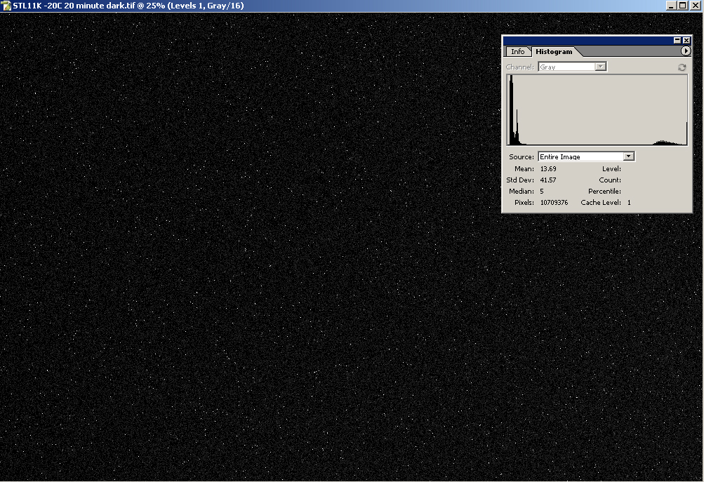
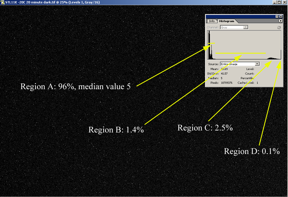
range. Here is a bias calibrated histogram of a dark frame from
my STL11000 taken at -20C for 20 minutes:
As shown below, the
histogram can be
divided into distinct regions
occupied by pixels with varying amounts of dark current. Region A
is comprised
of low intensity pixels that represent the most common pixel species
(96%). Pixels in this location have most of their full well
available to them. In fact, if you want to be even more accurate,
Region A is comprised of two populations of low dark current pixels,
but I didn't see the need to split it into Region A1 and A2 for the
purpose of this analysis. Regions B, C, and D represent pixels
with
varying degrees of higher dark current, but it is important to note
that collectively they comprise
only 4 percent of the total. Within this group is a population of
saturated pixels (Region D) or near saturated pixels (Region C). From a
dynamic
range standpoint, these pixels are essentially worthless to us, but
thankfully they comprise only 2.6% of the population. Region B is
comprised of warm pixels that have a non-uniform dark current.
Although they have the potential for capturing real signal, they only
constitute 1.4% of the total.
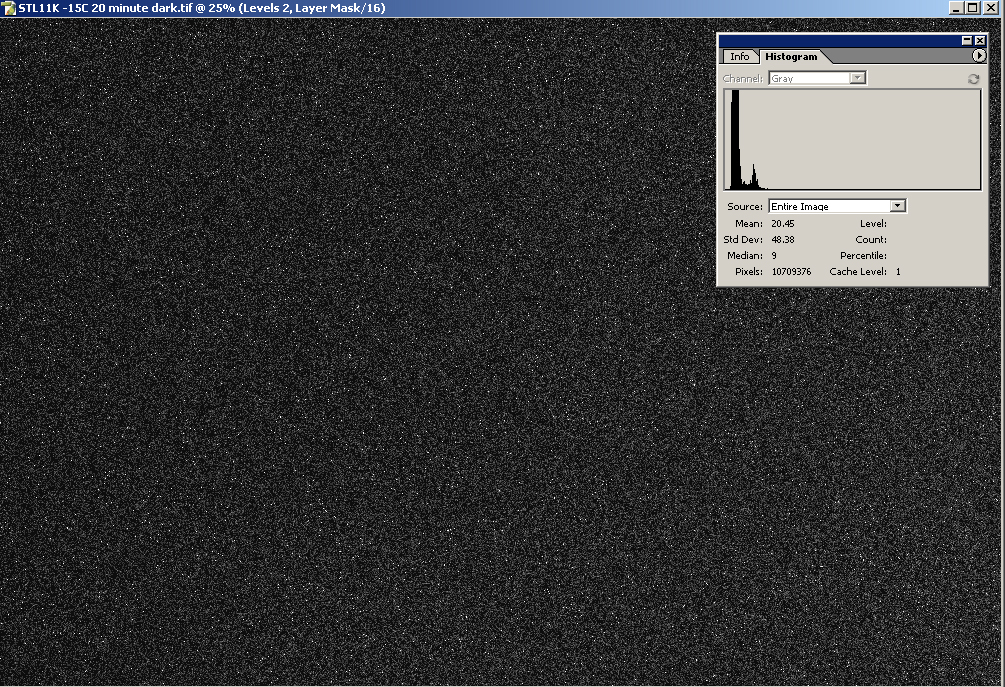
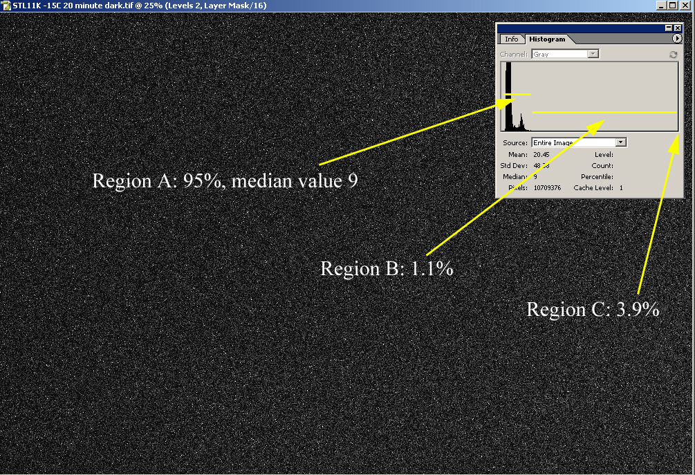
Here's what happens
when
you increase the
CCD temperature by 5 degrees. The figure below shows a
bias calibrated
histogram of a dark frame from my STL11000 taken at -15C for 20 minutes:
Notice what has
happened. Regions C
and D seen in the -20 degree histogram have now collapsed into one
saturated peak of clipped pixels that is difficult to appreciate but
is present as a thin line on the far right, comprising 3.9 % of the
population (Region C below). Region B is again comprised of
pixels with a non-uniform
dark current, many of which have the potential to accumulate real
signal, but
they only comprise 1.1% of the total. The
small fraction of pixels in regions B and C are part of the dark
signal
non-uniformity (DSNU), which is fixed pattern noise characteristic of a
given CCD chip.
Because they are always fixed in location, the effects of these higher
noise pixels on the signal to noise ratio can easily be eliminated by
dithering your images, followed by combining using a Sigma Reject
algorithm. For this reason, they are of minor consequence to the
signal to noise of the final image, and they will be ignored for the
purpose of this analysis. Again we see that
the
most functionally capable population of pixels, Region A, represents
95% of the total. Visually you can appreciate that Region A has
eaten
into the dynamic range a bit, since the median has shifted over to 9
(the median was around 5 at -20C). It is this shift that we will
be quantifying in our analysis of the relationship between dynamic
range and CCD temperature. In other words, the
distribution of pixel intensities in these dark
histograms make it reasonable to ignore the
small population of warm or hot pixels, and to focus our attention on
the bulk of the pixels on the left end of the
histogram,
which can be approximated by the average dark current equation
(Equation 9).
C)
Interactive Graphs:
Equation 13 allows
us to
graph the
functional dynamic range versus
CCD temperature under a variety of conditions. As before, here
are a few scenarios:
Example
1: Vary the Sky
flux.
Parameters as follows: R = 8 e RMS;
D0 = 30 e/minute/pixel at T0 = 0 degrees C; Td = 6.3 degrees C (D0, T0,
and Td characteristic of the KAI 11000 chip). Click on
the this link
to open a graph of Functional Dynamic Range (y axis) versus CCD temp (x
axis). The slider will vary the sky flux from 0 (e.g., the
Hubble) to 500 (a light polluted imaging
site) as it moves from
left to right (incremental steps of
10 e/min).
Notice how the functional dynamic range is affected by CCD temperature
in the range of -15 to -20 C at various sky flux values. When the
slider is all the way to the left (sky flux = 0; deep space), we see
that the achievable dynamic range is high, and that the benefit of
additional cooling increases until the CCD temperature reaches the
range of -40 to -50 degrees C, at which point it begins to
plateau. However, even with relatively small increments in sky
flux, the functional dynamic range begins to drop very quickly,
associated with a flattening
of the curve, such that very little gain
in the functional dynamic range is observed after achieving CCD
temperatures in the range of -15 to -20
degrees. Again, this can be predicted from Equation 13- as the
sky flux grows larger, it dominates both the numerator and the
dominator, thereby dimishing the influence of dark signal (and read
noise) on dynamic range.
Example
2: Vary the
Read
Noise. Same
parameters as in #1, but with a
fixed sky flux of 20
e/min (typical of my
site with the STL11K and a
6nm Ha filter).
Click on
the this link
to open a graph of Functional Dynamic Range (y axis) versus CCD temp (x
axis). The slider will vary the read noise from 2 to 15 as
it moves from left to right (incremental steps of 0.5 e RMS).
The influence of read noise on the shape of the curve is minimal in the
CCD temperature range of -15 to -20 C under these conditions.
Example 3: Vary the baseline D0
value
(i.e., the dark current specification of the chip at T0). Even
though D0 is a
characteristic of the chip as opposed to a variable under our control,
it is instructive to see how this parameter affects the functional
dynamic range. This
graph uses the same parameters as in
#1, but
with a fixed sky flux of 20 e/min (typical of my site with the STL11K
and a
6nm Ha filter). Click
on the this
link to open a graph
of Functional Dynamic
Range (y axis) versus
CCD temp (x
axis). The slider will vary the D0 value
from 1 to 50 e/min as it
moves from left to right
(incremental steps of 1
e/min). Notice the
profound effect that D0 has on the functional dynamic range at warm CCD
temperatures, but how immune the curve is to dark current once the chip
has been cooled to the -15 to -20 C range. In fact, even at a
chip temperature of 0 degrees C (which most of us would consider too
warm for imaging), a very low D0 value can support an excellent level
of functional dynamic range! A stated above, the KAF
16803 is typical of such a chip (with a D0 of 10 e/min at
T0 = 0 degrees C).
Bottom line:
As in the discussion involving the SNR, the influence of CCD cooling on
dynamic range is largely determined by imaging site (sky flux) and chip
characteristics (D0). CCD cooling beyond -15 to -20 C produces
minimal gains in the functional dynamic range for most imaging sites,
because the sky flux becomes the limiting factor in this situation
(graph in example 1). As CCD chips are manufactured with better
dark current characteristics (D0), the need for extreme cooling becomes
even less (graph in example 3). This is interesting, because when
the KAF 16803 chip was introduced into amateur astrophotography, it
seemed that the emphasis was on achieving even greater cooling,
when in fact these chips would be perfectly happy with less.
Nonetheless, it is important to note that the functional dynamic range
is optimized at very cold CCD temperatures under conditions of low sky
flux, such as one would find in deep space.
D)
Interactive Excel
Spreadsheet:
If you have made it this far,
you are either very committed, very
crazy, or both <g>. It is easy to calculate the
maximum possible functional dynamic range for a given set of
initial conditions, under the idealized situation in which the dark
current is zero. This equation would simply be equation 13, but
without the dark current term:
Equation 14.
Maximum Functional
Dynamic Range = [FW - (tsub*sky)] / SQRT[(tsub*sky)+R^2]
The
ratio of
actual functional dynamic range at a given CCD
temperature to the maximum possible functional dynamic range is then
obtained by dividing equation 13 by equation 14. I have made an Excel
Spreadsheet that
allows you to input initial conditions, state your desired CCD
temperature, and then determine how this affects your ability to
achieve the maximum possible functional dynamic range. You
will see that for most real world conditions of amateur
astrophotographers, being in a range of -15 to -20 degrees C allows us
to achieve a significant fraction of the maximum dynamic range.
Notice, however, what happens when you use a sky flux value of 0 (deep
space). Here is where extreme CCD cooling really shines, but
hopefully this analysis has convinced you that this is the exception
rather than the rule. You are welcome to experiment with
this spreadsheet to get a feel for the
numbers.
III.
Conclusions
I hope that you've had fun
with
this analysis. None of this is
intended to inhibit research and
development of better cooling systems by manufacturers of amateur CCD
cameras. The marketplace is an "arms race," and everyone is
trying to compete with each other to make the best products
possible. This is a good thing for consumers. But sometimes
an idea (like cooling) takes on a life of its own, such that we
automatically assume that we need the latest and greatest cooling to be
happy in this great hobby of ours. We sometimes place more
emphasis on the technical
characteristics of a camera, characteristics that have an over-inflated
impact on our images, and not enough emphasis on our own skills as
imagers. To be sure, if I wanted to build a camera to function on
board Cassini, you bet that I would want to cool it down as much as
possible. And if I lived in a very warm climate, I would want to
be confident that my camera was able to cool to the range of -20
degrees C
without too much effort. But given our skies, and especially
given the new revolution in low dark current CCD chips, I contend that
ground-based amateurs generally don't need cameras that can cool to -30
C to take great images. For the most part, we don't even need
cameras that can cool to
-25 C. And
by imposing more aggressive cooling on these chips, it is possible that
we are increasing the likelihood of experiencing other side effects
such as residual bulk image (RBI), although that is a topic for
another day.
If you enjoyed this analysis, I also
recommend that you check John Smith's cooling analysis,
which is very informative.